Better than Sliced Bread, "OmniProto" Boards Let You Make Anything!
Level Up Your Prototyping
I recently ordered something from JLCPCB that has changed my life forever. They have only been referred to as "advanced protoboards" until now, but they are so genius that they deserve a proper name. Seeing as it's not taken, I think OmniProto is a good one. Why? Because this protoboard can do damn near everything.
I'm hard pressed to even conceive of something that could be more useful for prototyping other than, like, a good soldering iron and inspection microscope if you don't already have those.
I'm never going back. I'm donating all of my stripboard, perfboard, and cheap protoboard to the local hackerspace. I'm an OnmiProto girl now.
Just look at this incomplete assortment of programmers and breadboard modules I've made with it:
 |
| Who needs breakout boards? |
Those were all made from a single 10 cm x 10 cm OmniProto, and over half of the board was left afterwards! Because you can make things so small, it takes a long time to use up even the minimum order size of 5 PCBs. Indeed, EVERYTHING you will see in this blog post was made from JUST ONE OnmiProto, with leftovers!
You can see a lot of things going on in that image. Through hole components, surface mount components, supernaturally helpful solder traces... what black magic is this? I wish I could say I was the mad wizard who came up with this idea, but that honor goes to "Electronic Eel" and their Open Source Advanced Protoboard. I re-created the pads in my own fork and added design blocks for EAGLE / Fusion Electronics so I could make my own sizes and shapes, or fill in empty space on an existing design with this wonderful pattern.
| This sight is usually the start of all your dreams coming true. |
So what makes it so special? Several things in tandem:
- It's twice the density of a standard protoboard, allowing SMD components with 50 mil (1.27 mm) pitch to get soldered right on without any fuss.
- It still has the standard 0.1 in (2.54 mm) breadboard-compatible holes that are essential in a protoboard. Standard breadboard components fit fine.
- The complex shapes of the pads allow you to contort all sorts of microscopic 2-6 lead components directly to the pads.
- The pad shapes allow adjacent connections to be easily made or broken, allowing you to draw 1.27 mm pitch PCB-like traces with solder (but only at a specific soldering iron temperature).
- Because the holes are through plated, they also act as vias, meaning moving signals to opposite sides of the board is a breeze. (This also means you sometimes need to avoid making traces over holes that already have a trace on the other side of the board, or they would be shorted.)
There is definitely some technique and skill associated with drawing good, non-shorting solder traces, but mostly you'll want to make sure your soldering iron is adjustable. You want to go a lot lower than you normally would, so the solder has more working time before the heat spreads down the trace and melts it all into a blob (that is, there is ANY working time as opposed to an instant solder mess). I use 60/40 leaded solder and normally set my AOYUE Int968A+ soldering station to 320C for regular soldering, but go down all the way to 250C for drawing traces on OmniProtos. Your temps may vary based on your iron, solder alloy, and tip.
Without further ado, let's get into some projects I've made with them so far! I have a lot of spare SMD parts from old work projects that I have never been able to use for prototyping until now, in addition to a bunch of old ATtyiny85's (both DIP and SOIC) just lying around that I want to do something, anything with. I also needed a SAM programmer for another project I'm doing. Let's take all those ideas and parts, then combine them with an OmniProto and some solder to make our dreams come true!
SAM Programmer + USB Breakout Fixture
 | |
| Oh god, it looks ugly. |
Okay, so the mess of wires you're looking at here is actually my programming and test fixture for a project I am developing, the world's smallest SAMD21 development board. It has no USB header by design, so for testing the USB functionality, I need to be able to solder a USB cable directly to the exposed pads around the edge of the board.
Speaking of USB, I need to flash the UF2 bootloader before that will work. I am able to do that with a MKR Zero, but it requires me to temporarily connect specific pins to the surface mount pads on the board edge.
What I made here is essentially a 2-in-1 breakout that both exposes a USB port as solderable wires and also connects the correct pins from a MKR Zero to a programming header I can hold at an angle against the pads to make good contact. (I call it a poor-mans pogo pin as the flex of the header pin gives the needed spring action, but it only works with a single row of pins.) The firmware file is stored on the microSD card, and I can verify that it programmed the board successfully over the serial terminal.
 |
| Stripped down. |
It's much easier to see the connectors when everything is removed.
 |
| Pinout |
Here you can see the 2 separate functions broken out onto different headers. Ground is not shared between them, as it was unnecessary.
 |
| Bottom |
Now you can clearly see that there are 2 completely separate circuits. Let's zoom in.
 | |||
| USB Breakout Section |
Nothing too crazy here, other than the fact that it's super simple to make these connections with nothing but some solder!
 |
| SAM Programmer Section |
Here is where I got my first taste of proper 1.27 mm traces. That pin 12 had to jump over it's neighbor!
 | ||
| Poor-Man's Pogo Pins |
Finally, here's a closeup of the programming header. Just a couple of male headers soldered back-to-back.
AVR Programmer - "Mezzanine" Daughter Board System
 |
| Now THAT looks sexy! |
Remember how I said I had a bunch of ATtiny85's lying around that I wanted to do something with? Well, I can't very well do anything with them if I'm unable to upload a program to them!
In the past, I have used various Arduino boards with the ArduinoISP sketch to enable them to work as AVR programmers. I've use breadboards with temporary wires, DIY shields for Uno and Mega boards with unreplacable DIP sockets that wear out eventually, and even hard-soldering a nano to a protoboard with a several different sizes of DIP socket to support different AVR DIP chips. All of these solutions were temporary, annoying, and not very reliable over time.
So this time around, I'm aiming to make the LAST AVR programmer I will ever need. It uses a Nano on pluggable headers, and breaks out the needed pins for power and programming to a single row header. This is not a standard 2x3 ICSP header because this way, it can be plugged directly into a mini breadboard, hanging off the side (good for quick power). Additionally, it enabled me to upgrade the board to also support a high voltage programmer option (more on that at the very end of the blog post).
The idea is that I might need different sockets wired to the same pins, such as DIP-8, DIP-14, pluggable headers for SOIC breakouts, etc. So I have a different daughter board for each use case, each with it's own special wiring to the "standard" header. I call the daughter boards "mezzanines", because they hang off the edge of the PCB in a way that looks kind of like a mezzanine. (Don't say engineers never did anything creative.) Pictured above is the DIP-8 mezzanine which I will get into later.
 |
| Stripped down. |
With the mezzanine and Nano removed, you can see the 10uF cap that's needed between Reset and GND for ArduinoISP to work.
 | |
| Pinout |
Here you can see the pinout. As with all my pinouts, I try to keep voltage and ground on opposite sides to avoid shorts. I also just ordered the pins to be most convenient when soldering, and also in a way that is easy to remember.
Let's call it the NIMAVR Programming Header, because why not?
 |
| Bottom |
Flipping the board over, we see the traces. Let's get closer:
 | |
| Microscope imagery of the bottom. |
Still nothing too crazy with this soldering. The most interesting thing is the 5V line crosses a trace using some holes as vias to pop over to the other side of the board and back.
DIP-8 Mezzanine + DIP-8 Header Mezzanine
 |
| They're twins! |
So my initial way of handling the NIMAVR to DIP-8 mezzanine was to solder a DIP socket directly to the board, connect the pins up to the NIMAVR header, then add the 0603 onboard LED (pin 1, or LED_BUILTIN). Sadly, I soon realized that to do SOIC-8 chips with the stuff I had lying around, I would need to reflow them onto a DIP-8 breakout board, which would INSTANTLY RUIN the IC socket if I tried to jam it in there. (Even putting the chip all the way in removes the spring from the pins after a few uses, so I normally just barely seat the pins.)
I realized I would have to make a second copy that does the exact same thing, but has different headers. This made me sad, and it made me realize there was a better way, but only once I made a version with pin headers. So that "better way" will be later in the post, for now, this is what I made to get the job done initially.
 |
| This PCB doesn't follow the DRY design principle... |
Yup, the same thing, repeated twice. Let's zoom in:
 | ||
| Let's play "Where's The LED?" |
Now you can actually see the tiny LED and resistor to the left of the boards. When I upload the default "Blink" sketch to the tiny, it makes that LED light up. It's a perfect test for making sure the chip is programmable and that the clock is running the correct speed.
 |
| Spot the difference! |
On the left one, I actually had to do some pretty tricky rework. For the first time, a pad got ripped up! I have been REALLY abusing these pads for some time and they never came up before this, but maybe I heat cycled it a few too many times or something. Either way, here is a close-up of that absurdly tiny fix.
 |
| Nailed it. |
USB B Breakout Board
 |
| Wait, didn't we see this already? |
So I know, I already made this on the SAMD programmer. But I wanted a small standalone version that I could pop in a breadboard. Easy 5V power right there!
 | ||
| Pinout |
Just the standard USB A pinout.
 |
| Bottom |
Just some traces, you've seen it all before.
4 LED Breakout Board
 | |
| Now we're thinking with SMD! |
One of the most annoying parts of prototyping on breadboard is setting up LEDs. They take up a ton of space, get in the way when trying to place or route things, you need to connect each and every one to a resistor and ground... it's annoying to say the least. Often, I just want to see what my GPIO pins are doing WITHOUT filling half my breadboard with LED circuits.
I made this to solve that problem. It has 4 LEDs, each with a 1k resistor and the cathodes hooked up to ground. It hangs off the side (over the voltage rails) so it takes up nearly no precious space on your breadboard.
 |
| Pinout |
Other than GND, each pin lights up the LED next to it. The labels are arbitrary.
 |
| CLEAN |
I think this is actually beautiful. You can visually see the whole circuit WHILE it's plugged into the breadboard. There's no guessing which pin does what, just look at it and find out.
Tiny Time! Capacitive Touch Experiment
It was around this time I was getting antsy to *do* something with an ATtiny85, so I googled around for cool projects people made with them. I found one where someone abused the ADC to act as a capacitive touch sensor... somehow. You can read up on how it works here, but all I care about it is how well it works.
In my example on a breadboard, it worked great! So I tried to make it on OmniProto.
Before you look at this next image, I have a confession. The LED breakout I showed you earlier started life as this capacitive touch module. Because of the extreme stray capacitance of the PCB, it straight up didn't work no matter what I did. So I took the LEDs I had so nicely put on the outputs and extracted them from this failed design.
 |
| Bottom |
Here you can see a SOIC-8 ATtiny85v, a resistor, and some traces to the headers.
 |
| Top |
There are those LEDs on the output, and the solder blob up top was supposed to be the touch pad. Well, it's a pad, and I touched it, but nothing happened. Time to grab the solder wick and try something else.
AVR Programmer Revised - High Voltage Programmer
 |
| Achievement Unlocked: Getting an Upgrade |
So the ATtiny85 is actually really powerful, but the main limitation is that it only has 5 GPIO pins to work with. Well, that's not entirely true, as it IS possible to reconfigure the reset pin (pin 1) to be GPIO pin 5 using fuses... but that means that it won't work as a reset pin anymore! Since the reset pin is used for programming, that would mean the chip would never be programmable again! That is true, unless you have a programmer that can use 12V signals on the reset line! You can make one of these programmers using a Nano, but it requires 2 more pins than the standard ArduinoISP sketch. Additionally, you need 6 resistors, 1 NPN transistor, and a 12 volt source.
I modified my existing AVR programmer to support the 2 extra GPIO pins, then made a high voltage programmer mezzanine using an MBT2222A NPN transistor I had from an old project and a barrel jack for an external 12V source. Additionally, having to unplug the Nano each time I needed to swap between ArduinoISP and the high voltage fuse burning sketch due to the 10uF cap was annoying, so I installed a switch that connects and disconnects the cap.
 | |
| Stripped down. |
With the other stuff removed, we see everything clearly.
 |
| Pinout |
The same pinout as before, but with some new GPIO. Note how the connectors have a gap, signifying that the left part is an addition to an existing connector.
 |
| Bottom |
Flipping the board, we see the new traces.
 |
| Microscope imagery of the bottom. |
Nothing too fancy here. Let's move on to the mezzanine.
 |
| That's a busy protoboard! |
Now THIS is fancy! We'll get a closer look at some of the tricks I pulled on the top in a moment. First, check out the bottom.
 |
| OH YEAH, that's the good stuff. |
I won't even attempt to lie, I'm proud of this. Some parts look sloppy, but that's because I had to rework them 20 times. I learned so, so much about soldering OmniProto with this one.
Let's take a closer look at the top now.
 |
| Approaching the density limit. |
My favorite bit about the top is the rework wires. The signals density was too high in that area and I had nowhere to route the traces, so I took some rework wires and made some floating traces! I even anchored the longer one in the center to ensure it wouldn't move a millimeter!
It's also nice to see the extra components basically hidden amongst the solder traces. Even though it's a ball of solder blobs, somehow it still feels like a really clean solution.
 |
| Drawing with solder like a Sharpie. |
Do I even need to say anything about this? Just look at it. LOOK AT IT! Tell me of a single other protoboard design that can do anything CLOSE to that!
I love OmniProto, man.
DIP-8 to Pin Header Breakout Board
 |
| The Better Way |
You may have noticed that the high voltage mezzanine has pin headers, and no way to program DIP chips. You may have wondered if I was going to do that insane solder job a second time, like I did with the first mezzanine. Nope, no way! Instead, I threw the DIP mezzanine I made into the junk drawer and made a pin header to DIP adapter. This seems obvious in hindsight, but isn't that just how it goes?
 |
| Bottom |
It's a really simple board. If I ever have to make more, I won't mind very much. Now I don't have to worry if I wear out my DIP sockets! (At least until I can afford REAL programming sockets.)
 |
| Side |
For this board, a side view gives more clarity than the microscope would. Really using the via functionality here and nothing else.
Here are some pictures of it in action.
 |
| High Voltage Programmer |
 |
| Low Voltage Programmer |
Tactile Button Breakout Board
 |
| Finally! Compact buttons on a breadboard! |
Yeah boi! Guess who found some tiny tactile babies in some old prototyping assortment kits? THIS GIRL! Just like LEDs, tactile buttons are a nightmare on a breadboard. They pop out all the time, take up WAY too much space, and need all these extra jumpers. I JUST WANT TO INPUT GPIO SIGNALS, BRO.
Since most of the time they are switching to ground or VCC anyway, I simplified 4 buttons into this tiny 5 pin breakout that hangs off the side of the breadboard, over the power rails.
 |
| Pinout |
Just like with the LEDs, the labels are arbitrary, and the pins match up to the button nearest to them.
Technically, you can put any signal on the shared pin, not just ground. I'm not your mom, I won't complain.
 |
| Close-Up |
OmniProto makes breakouts like these as simple as having the parts and some solder!
Single Schottky Diodes

What can I say? I needed to use some schottkys on a breadboard, but I only had SMD. OmniProto can build even your dumbest dreams!
 |
| Not For Human Consumption |
A closeup, anyone?
 |
| Smallest PCB I've ever made. |
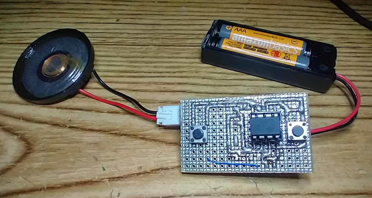
Case Study: Yes/No Button (from Bluey) Prototype
 |
| A Solid, Small, and Functional Protoype! |
The AAA battery holder is temporary, as I don't have a CR1220 battery yet. (I did have the holder for some reason...) The speaker will eventually be soldered directly to the board. So in all the following pictures, just imagine the white Molex connectors don't exist, a button cell battery is in that holder, and the speaker is soldered on somewhere convenient for installation into the yet-to-be-made 3D printed case.
 |
| I SAID IGNORE THE CONNECTORS |
Here you can see the battery holder and the audio amplifier module. While I could have taken the components off of the module and put them onto the OmniProto, that would have actually made it less compact, so I just soldered it onto headers that I trimmed after soldering. That blue wire is connected to the shutdown pin on the amplifier chip, as it wasn't broken out on the PCB and I wanted to turn the amp off when the chip was asleep.
 |
| Front |
Here you can see that rework wire go through one of the holes and over to the MCU. Speaking of the MCU, notice how I bent the DIP socket pins and surface mounted them BETWEEN the holes on the board! That allowed me to surface mount the battery right on the other side of the board!
There are also several RC filters scattered around for cheap DAC functionality and button debouncing. Lastly, there is a single volume control resistor (forms a DC voltage divider alongside a lowpass filter).
Let's get one last closeup. I had to skew this pretty bad to make the images overlap, fair warning...
 |
| I swear it's not bent in real life. |
Somehow, I think my phone camera got a better picture of this one than my thousand dollar microscope.
Oh well, here's a side view so you can see how compact I was able to make it.
 |
| Without the white connectors, it's tiny! |
Just look at that. If I could have made prototypes like this back when prototyping was my main gig, well, I would have struggled a lot less and had a lot more fun! Often I needed to order simple PCBs just because I needed to use SMD components, or to fit everything in a tight space, but with OmniProto, I could have probably shipped at least a few products without ever ordering a special board!
Anyway, I'm going to develop this into a Tindie product. If you want the code to make your own before then, here you go.
Now Go Forth and Make Anything!
Easy, place an order with your PCB house of choice! I use JLCPCB because they are cheap, fast, and reliable. If you need higher quality features than the bottom-of-the-barrel PCB, you can pay a little extra for them. For OmniProto, you can just use their $2 special. Upload this file to their website, it will give you options about how you want the boards made. Leave everything default to get the $2 deal. (You do get some choice of PCB thickness without changing the $2 price point if you want.)
I am aware that the pads on this design may become short circuited during the HASL process. Due to the way this board will be used, I do not care if short circuits occur, and I would like to proceed with the HASL process. Even if there are many short circuits on this board, I will still be 100% satisfied with my order.

Comments
Post a Comment